Board index › Projects › Floppy Audio Project

Encasing Blueprints

13 posts · 33109 views

Encasing Blueprints

by Paleorama » Wed Dec 07, 2011 20:04 UTC
Hi again,

I've been spending my spare-time contemplating a diagram with the needed buttons, knobs and various chips for turning the floppy drive into a complete instrument with a casing.

It looks like this (click for full size):
image

The first thing I've added, in the lower left corner, is 3-pole switch which cuts the connection to the power supply, turns off pin 14, and has an LED for letting one know when the bastard is turned on.

To the right is two switches directly connected to the floppy-connector-cable - one to 10/5 for turning on the motor, another to 18/9 for the direction of the stepper motor.

Above is a 555-timer IC, with resistor- and capacitor-values that makes the timer generate pulses in the 60-180 bpm domain. I found these quite useful for music-oriented tempi. I might experiment with the values when I get this converted to the real world.
A 2-pole switch lets one choose between the 555-pulse or a temporary push-button for one step at a time (this one I'm not sure if is correctly wired up?)

In the top left corner is another 555-timer. The fixed values of the components should generate a ~40 kHz signal.
This signal is meant for the bias-signal, which should erase the disk given a high enough amplitude.

I found an OP-AMP IC (TDA2822) which should be good for stereo signals. I want to build 2, one for the input signal, one for the output.

Given the fact that the heads on the FDD takes the input signal through the same lines as the output, I've drawn a 3-pole double throw-switch for the stereo signals plus the ground line. It lets one decide wether to record to the disk or play from it.

The last thing I've added is 3 LED's for the digital outputs on the FDD-cable, they should be lit when the drive detects the track 0 position, write protection I/O and Disk Inserted.

I'd very much like to receive feedback on this diagram! The OP-AMPs aren't yet drawn completely. I guess it should be quite straight forward.

Re: Encasing Blueprints

by Paleorama » Wed Dec 07, 2011 20:07 UTC
Here's the scheduled design, encased. I've thought of making a plexi-glass piece which lets one see the stepper motor in action. The rest should be self-explanatory. Cheers!

image

Re: Encasing Blueprints

by guest » Thu Dec 08, 2011 02:50 UTC
thats looking really good

be sure to put mixing resistors on the opamps

the rec/play switch probably only needs to be dpdt
as the ground can be shared by both circuits
same goes for the power switch
which only needs to disconnect one of the power lines
to break the connection

do pins 7 and 14 need to be disconnected when the power is off?

do the i/o and dir pins need pullup or pulldown resistors?

and it might be good to put some sort of lowpass filter
or other glitch rejection
on the pulse button
as pushing the button once
might cause many little spikes and step more than one step

Re: Encasing Blueprints

by Paleorama » Thu Dec 08, 2011 07:10 UTC
hi, thanks for your reply!

Yeah, I just realized it when I posted the pics. It's true that it's not necessary to break the ground connections!
So only DPDT switches are needed.

I thought it would be convenient to have Drive 0 turn on/off when along with the power. Just saving a switch and personal preference. Are you having some sort of problem with the 3PDT switches? :D

Regarding the motor I/O pin, I always just put it to LOW to turn it on - I dunno about the direction pin, if the switch could just go the power ground. Do you have a better suggestion?

But I absolutely agree with you on the pulse button! I read that it should have it's own circuit for preventing "mechanical extra pulses". It was actually pure laziness which made me leave this one out. Will look into it right away.

Thank you so much!

Re: Encasing Blueprints

by mcanulty » Sun Dec 18, 2011 08:06 UTC
Hey, I've been deep in a project at work and am only just now seeing all these posts, they are super impressive! Debouncing that switch probably wouldn't hurt, a quick search turned this page up, in case you are not sure what to search for to find useful approaches: http://ikalogic.com/debouncing.php It's a simple fix, but you'd be surprised what big problems it can cause if you forget about it. There are some fun horror stories, microcontroller guys tend to like to collect those kinds of stories I think.

But yeah, wow, I'm glad you're making so much progress!

Re: Encasing Blueprints

by mitcho » Mon Jan 23, 2012 19:20 UTC
I just made the circuit Paleorama posted with some changes: here's the eagle image
http://img857.imageshack.us/img857/8995/fddaudio.png
I use the max4548 analog switch to switch the signal to the FDD heads or from it. The L2722 is actually the L2822, but I couldn't find it in the library for eagle.
Well, the circuit has a problem: the signal that comes into the max4548 sounds like in a sinusoidal envelope. It comes and goes at different intervals from a couple of seconds to less then a second. When I took off the 555 chip there was no envelope anymore. Could anyone find out the reason for this or even better a solution? :D
here is also a photo of my circuit, it's already without the 555
image

thanks

Re: Encasing Blueprints

by guest » Tue Jan 24, 2012 10:41 UTC
first off id like to say that your board looks awesome
did you etch the pcb yourself?

i was looking at the schematic you sent
and i was wondering if all of the footprints are correct in there
for example
none of the opamps have a dc feedback path

ill see if i can locate some pictures of what it should look like

Re: Encasing Blueprints

by mitcho » Tue Jan 24, 2012 11:50 UTC
Thank you, yes I etched it with the help of a friend. I know the DC feedback is missing from the eagle schematic, but when I generate the board the DC shows up. I can hear the input amplified by the 2822(2722), so it works. The problem is still the 555. I even tried to measure the output frequency with a multimeter but seems that it is not working at all. I'll go check the board now, to make some more measurements.

Re: Encasing Blueprints

by guest » Tue Jan 24, 2012 12:06 UTC
what are the plus and minus supply voltages to the opamps?

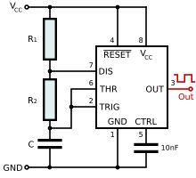
it looks like pin2 and pin6 on the 555 are connected wrong
check out this picture and compare
image

also
the 555 often needs a pullup resistor on the output
so a 1k from pin3 to Vcc should be fine

Re: Encasing Blueprints

by mitcho » Tue Jan 24, 2012 15:51 UTC
Wow, thank you so much for this, it works now, the 555 generates a frequency between 34 and 35 kHz, even without the pull up resistor (I haven't put it on yet, because it will take time and patience to solder it on this circuit). Now I have to write the program for arduino to serially control the analog mux max4548. I'll keep you up to date.

EDIT: the op amps I'm using need only positive voltage (5V). In fact, the chip they are in (the TDA2822M) is a dual amplifier and needs only positive voltage (min 1.8V, max 15V).

Re: Encasing Blueprints

by guest » Tue Jan 24, 2012 16:20 UTC
you may not need the pullup resistor
so if its working without it
dont worry

if youre running the opamps off a single supply
do you have any bias setting resistors
to move the voltage up to 1/2vcc

Re: Encasing Blueprints

by mitcho » Tue Jan 24, 2012 17:50 UTC
hmm... no.. i just went after this schematic
image
taken from the TDA2822M datasheet http://www.datasheetcatalog.org/datasheet/SGSThomsonMicroelectronics/mXqwxzy.pdf

Re: Encasing Blueprints

by guest » Wed Jan 25, 2012 10:11 UTC
i had looked up the wrong datasheet
that circiut is fine for small input signals

the datasheet also listed a bunch of other chips
that are used in portable cassette players
perhaps they would be useful as well